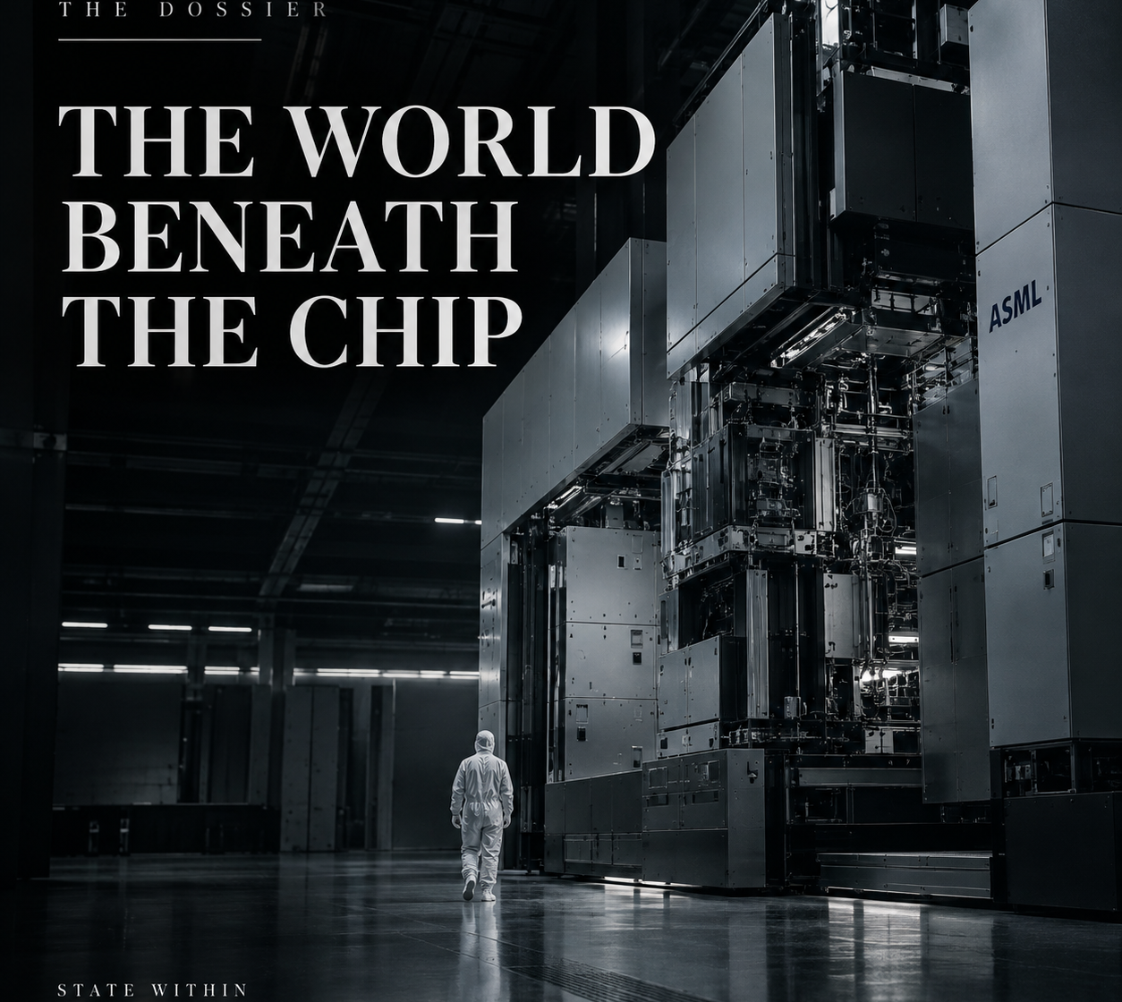
The finished object hides almost everything that matters. A processor does not show the software used to design it, the lithography system that patterned it, the chemicals that cleaned the wafer, the memory placed beside it, the engineers who learned how to manufacture it reliably, or the water and electricity that kept the factory running. It does not reveal how many borders were crossed before it existed.
This is why semiconductors have become an unusual object of geopolitical competition. They sit inside phones, cars, factories, communications networks, data centres and weapons. They enable artificial intelligence, while the expansion of AI increases demand for some of the most difficult parts of the semiconductor chain. Governments now subsidise factories, restrict exports, scrutinise investment and negotiate with allies over technologies that were once discussed mainly by engineers and corporate supply chain managers.
The familiar summary says that the United States leads chip design, Taiwan manufactures much of the most advanced logic, South Korea is central to memory, Europe possesses critical lithography technology, Japan supplies important materials and equipment, and China brings enormous manufacturing scale.
All of that is useful. None of it explains the system.
No country controls semiconductors as a whole. Different countries and companies possess different capabilities, and the strategic importance of those capabilities depends on how difficult they are to replace.
To understand where power sits, we have to go beneath the chip.
1. FROM DESIGN TO SILICON
The word chip covers technologies that perform very different jobs. Logic processors perform computation. Memory stores information. Analog devices connect the physical and digital worlds. Power semiconductors manage electricity. Microcontrollers operate machines that may never require anything close to the computing power of an AI accelerator.
This matters because semiconductor competition is often described as a race towards the smallest manufacturing process. Leading edge logic is certainly important, especially for artificial intelligence and high performance computing. Much of the modern economy, however, depends on devices produced with older technologies.
Cars require controllers, sensors, analog components and power electronics. Industrial equipment relies on devices chosen for reliability and long service life. Electrical systems need semiconductors designed to handle power rather than maximise transistor density. A component can be technologically unremarkable and economically critical if a production line cannot operate without it.
The shortages that followed the pandemic demonstrated this clearly. Relatively inexpensive chips could interrupt production of products worth tens of thousands of dollars. Sophistication and strategic importance are not the same thing.
The industry is also large enough that semiconductor disruption can no longer be treated as a specialist problem. The Semiconductor Industry Association reported worldwide sales of $791.7 billion in 2025. Logic accounted for $301.9 billion and memory for $223.1 billion. The association expected global annual sales to approach one trillion dollars in 2026.
Before any of those products can be sold, an international chain has to work.
Engineers need electronic design automation software and semiconductor intellectual property. Equipment manufacturers build lithography, deposition, etching, cleaning and inspection systems. Those machines depend on precision optics, lasers, sensors, components and software. Fabs consume wafers, industrial gases, highly purified chemicals, water and electricity. Fabricated dies then have to be packaged and tested before they can enter phones, vehicles, industrial systems or data centres.
Every stage has its own suppliers and geography.
The design stage is particularly revealing because its dependencies are difficult to see. Companies such as Nvidia, AMD, Qualcomm and Apple can design sophisticated processors without owning the factories that manufacture them. Foundries specialise in converting those designs into silicon. This division allowed enormous specialisation, but it also made software and intellectual property industrial inputs.
A country can therefore build a fab while remaining dependent on foreign design tools and engineering ecosystems. Those dependencies do not appear on a satellite image, but they can be just as real as dependence on a factory.
Materials create another layer.
Silicon remains the foundation of most semiconductor production, but fabrication uses a much wider collection of inputs. Gallium compounds matter in radio frequency, optoelectronic and power applications. Germanium has specialised uses. Hafnium is used in advanced transistor structures. Copper is fundamental to interconnects. Photoresists, fluorine related materials and industrial gases have to meet demanding purity requirements.
This is why the phrase critical minerals needs care. A mineral deposit is not the same thing as a technological input.
Gallium, for example, is generally recovered as a byproduct. The relevant chain runs through recovery, refining, purification and industrial qualification. A country may possess geological resources without possessing competitive processing capacity. Reopening a mine can therefore leave the more difficult parts of the problem unresolved.
China’s position in several material chains has attracted growing attention for precisely this reason. Beijing introduced export licensing requirements for gallium and germanium products in 2023 and later expanded controls into other strategically sensitive materials. The significance of those measures depends on the material, the application and the time required to establish alternative supply.
The semiconductor chain is already global before a wafer enters a fab.
2. THE MACHINES
If design software represents one of the industry’s least visible dependencies, semiconductor manufacturing equipment represents one of its most physical.
The most striking example is extreme ultraviolet lithography. EUV uses light with a wavelength of 13.5 nanometres to pattern extremely small features on wafers. Producing that light requires powerful laser pulses to strike microscopic droplets of tin, creating plasma that emits EUV radiation. The light is absorbed by air, so the optical path operates in vacuum. Conventional lenses cannot perform the required task, which means the system depends on exceptionally precise mirrors.
ASML is the world’s only commercial manufacturer of EUV lithography systems. ZEISS is the exclusive supplier of the optical systems at their core. Their work sits inside a supplier network built over decades.
The scale of the newer High NA generation shows why the capability cannot be reduced to the price of a machine. ZEISS says its projection optics contain more than 40,000 parts and weigh around twelve tonnes. The metrology equipment used to measure the mirrors weighs roughly 150 tonnes. Some mirrors take about a year to manufacture.
Reproducing such a system would require more than obtaining drawings. It would mean reproducing precision manufacturing, metrology, specialised suppliers, software and accumulated knowledge.
Lithography is only one equipment category. Fabs also require deposition, etching, ion implantation, cleaning, thermal processing and inspection. Companies including Applied Materials, Lam Research, KLA and Tokyo Electron hold important positions in different parts of this market. Supplier concentration varies by tool, which is why semiconductor equipment should not be described as a single chokepoint.
The broader pattern is nevertheless clear. A country can possess capital, engineers and a desire to manufacture advanced chips while remaining dependent on equipment produced by a small number of companies elsewhere.
3. THE FACTORY IS LARGER THAN THE FAB
Eventually the design has to become silicon. This is the part of the industry that attracts the most political attention because a fabrication plant is visible, expensive and geographically fixed.
It is also easy to misunderstand.
A modern fab is not a building in which the correct machines have simply been installed. Manufacturing depends on process recipes, maintenance, metrology, supplier support, engineering judgement and years of operating experience. Identical equipment does not guarantee identical yield.
TSMC gives a sense of the scale. In 2025 the company manufactured 12,682 products using 305 process technologies for 534 customers. Its annual capacity exceeded 17 million twelve inch equivalent wafers. Technologies at seven nanometres and below generated 74 percent of wafer revenue, while two nanometre technology entered high volume manufacturing in the final quarter of the year.
The company is expanding well beyond Taiwan. Its first Arizona fab entered high volume production on N4 technology in late 2024. A second is being equipped for more advanced production and is expected to reach high volume manufacturing in the second half of 2027. Japan and Germany are also becoming part of TSMC’s wider manufacturing network.
At the same time, TSMC continues to expand advanced production and packaging in Taiwan.
Geographic diversification does not reproduce an industrial ecosystem overnight. New fabs need engineers and suppliers. Equipment has to be installed, calibrated and maintained. Processes have to be qualified. Yield has to improve until production is competitive at scale.
Packaging adds another layer that has become increasingly important with artificial intelligence.
Advanced computing systems combine processors, memory and specialised dies inside complex packages. TSMC has developed technologies including CoWoS, InFO and SoIC. Intel uses approaches including Foveros and EMIB. Packaging has become part of system design rather than simply the final protective step around a finished die.
High Bandwidth Memory makes the change particularly visible. HBM stacks DRAM to provide the bandwidth required by AI accelerators. By 2026 Samsung and SK hynix were shipping their HBM4 generation, while Micron was expanding HBM production and packaging capacity.
New capacity takes time. Micron expects a new Singapore HBM advanced packaging facility to contribute meaningfully to supply from 2027. SK hynix broke ground in Indiana in August 2026 on a facility involving more than four billion dollars of investment, with mass production targeted for the second half of 2029.
A leading edge processor can therefore exist while the final computing system remains constrained by memory or packaging capacity.
The fab also depends on infrastructure that rarely appears in semiconductor headlines.
Intel says a fab can consume nearly four million gallons of water per day. TSMC reported global water consumption of 151 million cubic metres in 2025. Its Taiwan operations were using more than 67,000 cubic metres of reclaimed water each day, and cumulative reclaimed water use had exceeded 23.5 million cubic metres by the end of that year.
Electricity is equally fundamental. Fabs operate continuously and contain large numbers of energy intensive process tools. Reliability matters alongside volume because a serious interruption can affect work in progress and require complex recovery procedures.
People form another constraint. A study by the Semiconductor Industry Association and Oxford Economics estimated that the American semiconductor workforce could grow from roughly 345,000 to 460,000 by 2030, while around 67,000 new technical positions could remain unfilled at prevailing education and training rates.
The problem is not simply headcount. Semiconductor manufacturing contains tacit knowledge acquired through operation, troubleshooting and process improvement. Some of that knowledge can be documented. Much of it is learned by teams over time.
This is why a fab cannot be recreated by capital expenditure alone. The factory extends into its suppliers, infrastructure and workforce.
4. A MAP OF DEPENDENCIES
Once the industry is separated into capabilities, the political map becomes less useful.
The United States is exceptionally strong in design, electronic design automation, intellectual property and several important categories of manufacturing equipment. South Korea holds a central position in memory. Japan remains important in materials and equipment. Europe contains critical equipment and precision optical capabilities. Taiwan is central to advanced foundry manufacturing and advanced packaging. China combines enormous electronics manufacturing scale with a large share of installed wafer fabrication capacity and substantial assembly, testing and packaging activity.
These are different measurements. Value added in design cannot be compared directly with installed wafer capacity. Total wafer capacity does not reveal how much can manufacture the most advanced logic. The location of a corporate headquarters does not tell us where every production step occurs.
Analysis published by the Semiconductor Industry Association and Boston Consulting Group illustrates the specialisation. In its 2024 activity map, the United States accounted for about 66 percent of value added in intellectual property and electronic design automation and 73 percent in logic. South Korea accounted for about 63 percent of memory. Equipment value added was divided mainly among the United States at 41 percent, Japan at 24 percent and Europe at 24 percent.
The fabrication map looked different. China accounted for 27 percent of installed wafer capacity, Taiwan 18 percent, South Korea 16 percent, Japan 15 percent, the United States 10 percent and Europe 8 percent. Assembly, test and packaging followed another distribution again.
The semiconductor industry is therefore not a hierarchy with one country at the top. It is a network of specialised positions.
That network is now being examined not only by companies managing cost and supply risk, but by governments looking for vulnerability and leverage.
5. WHERE THE SYSTEM NARROWS
Concentration alone does not create a strategic chokepoint.
A capability becomes more consequential when few suppliers can provide it, substitutes are weak, replacement takes a long time, alternatives cannot scale quickly and access can actually be restricted. The downstream effect of disruption matters as well.
EUV lithography satisfies these conditions unusually well for leading edge manufacturing. ASML is the only commercial supplier of EUV lithography systems and ZEISS supplies the critical optical system. Reproducing the capability would require far more than building another expensive machine. It would require recreating a supplier network, precision manufacturing, metrology, software and decades of accumulated knowledge.
Leading edge foundry manufacturing is also highly concentrated, although it is not a single supplier market. TSMC occupies the strongest position, with Samsung and Intel providing other advanced manufacturing paths. Building competitive capacity requires enormous capital and years of process learning, which makes short term substitution difficult.
Electronic design automation and selected categories of manufacturing equipment create other narrow points. Their supplier structures differ, so neither should be treated as one homogeneous market.
Artificial intelligence has added HBM and advanced packaging to the list of capabilities that deserve close attention. Their importance is application specific. HBM can constrain frontier AI systems while having little relevance to a household appliance or many automotive components.
Materials are even more varied. Some are highly concentrated, some have credible substitutes and some can be produced elsewhere if enough time and money are available.
A useful map of semiconductor power therefore changes according to what is being built and how long the system has to adapt.
6. TAIWAN
No place demonstrates the semiconductor system’s concentration more clearly than Taiwan.
Its importance is often compressed into a single statistic about the share of advanced chips manufactured there. Many versions of that statistic still circulating in public debate come from older estimates. The more durable fact is the industrial cluster itself.
Taiwan contains advanced fabs, packaging capacity, suppliers, experienced engineers and decades of manufacturing knowledge. TSMC sits at the centre of that system, but the strategic asset is larger than one corporation.
The company is diversifying rapidly. Arizona is becoming a multi fab manufacturing cluster. Japan is expanding from specialty technologies towards more advanced production. Germany is adding automotive and industrial capacity. Yet TSMC is also building multiple phases of two nanometre capacity in Taiwan and continuing to invest there in advanced packaging.
This is why the idea that overseas fabs simply move the Taiwanese semiconductor ecosystem elsewhere is misleading. They reduce particular geographic risks and add valuable capacity. They do not instantly reproduce the density of suppliers, engineering experience, infrastructure and production knowledge that developed around Taiwan over decades.
This also complicates the argument sometimes described as Taiwan’s silicon shield.
One view holds that semiconductor interdependence discourages conflict because disruption would impose enormous economic costs on China, the United States and much of the global economy. Another holds that strategic importance can increase the value of coercing, controlling or denying access to an asset.
Semiconductor data cannot establish which effect is stronger.
Military invasion is not the only relevant risk in any case. A blockade, quarantine, cyberattack, earthquake, electricity disruption, water shortage or logistics failure could affect production in different ways and for different lengths of time.
The useful question is therefore not whether chips make Taiwan safe. It is how much of the global system can continue operating if access to Taiwanese capability is interrupted, how quickly alternative production can respond and which products are affected first.
That is the problem governments are now spending extraordinary amounts of money trying to reduce.
7. WHEN DEPENDENCE BECOMES LEVERAGE
The semiconductor industry was international long before governments began treating it as a strategic contest. What changed was the way they learned to read the network.
A supply chain built for efficiency can reveal dependence. If an essential capability is concentrated, difficult to substitute and subject to a government with the practical ability to restrict access, commercial centrality can become political leverage.
American semiconductor export controls show how this can work.
The controls introduced in October 2022 and expanded later did not attempt to prohibit every semiconductor transaction with China. They focused on particular advanced computing capabilities, manufacturing equipment, software and end uses. In December 2024 the Bureau of Industry and Security added controls affecting 24 types of semiconductor manufacturing equipment, three categories of software tools and high bandwidth memory, while adding 140 entities to the Entity List and modifying other restrictions.
The choice of targets matters. A government interested in constraining a technological capability does not necessarily need to control the finished product. It can look upstream for the things required to produce it.
American law can also reach beyond goods physically manufactured in the United States. Under defined circumstances, foreign produced items that are the direct product of specified American technology or software can fall within American export rules. This gives regulatory importance to the country’s position in design tools, equipment and technology.
In August 2025 Washington ended license free Validated End User treatment for selected foreign owned semiconductor fabs operating in China. The Commerce Department said it intended to allow licensing needed to operate existing facilities but not to support capacity expansion or technological upgrades.
The distinction is significant. Economic statecraft does not require an immediate shutdown. Restricting the speed at which a competitor can approach the technological frontier can itself have strategic value.
The idea often described in academic literature as weaponized interdependence is useful here if it is used carefully. Interdependence is not inherently coercive. It becomes a source of leverage when a network contains difficult to replace nodes and an actor possesses both control over access and the institutional ability to use it.
China has been mapping the same chain from the other direction.
Beijing has supported domestic fabrication, equipment, memory and design while encouraging substitution for foreign technologies. Chinese firms have expanded mature process capacity and pursued more advanced manufacturing under tighter access to some foreign equipment.
China also holds concentrated positions elsewhere in the industrial system. Gallium and germanium are useful examples. Export licensing requirements were introduced in 2023 and controls later expanded into other sensitive materials. The United States Geological Survey reported that in December 2024 China prohibited exports to the United States of certain dual use items related to gallium, germanium, antimony and superhard materials and strengthened controls affecting graphite.
These measures are not the mirror image of American restrictions on advanced semiconductor technology. Gallium is not EUV lithography. Supplier structures, inventories, substitutes and replacement times differ.
The common feature is the method. Both sides are identifying places where the other depends on capabilities that may be difficult to replace quickly.
The same map that helps a company manage procurement risk can therefore help a government identify leverage. Once that happens, reducing dependence becomes an industrial policy objective.
8. REBUILDING THE CHAIN
Governments are now paying to create additional semiconductor capacity, move production, train workers and reduce reliance on concentrated foreign suppliers.
The sums are large. Final United States CHIPS awards announced in 2024 included up to $6.6 billion in direct funding for TSMC’s Arizona expansion, up to $7.865 billion for Intel, up to $4.745 billion for Samsung and up to $6.165 billion for Micron. Amkor received an award of up to $407 million for an advanced packaging and testing project in Arizona.
Europe is pursuing a related strategy. The European Commission says the original European Chips Act helped mobilise more than €52 billion in public and private investment. In February 2026 the NanoIC pilot line opened at imec in Belgium with €2.5 billion in total investment, providing access to advanced EUV infrastructure for research on technologies below two nanometres.
The Commission proposed a second Chips Act in June 2026. Its language is notable because it does not promise semiconductor self sufficiency. The emphasis is on reducing strategic dependencies while strengthening European capabilities and preserving important positions in global supply chains.
Japan is attempting a return to leading edge manufacturing through Rapidus. By February 2026 the Ministry of Economy, Trade and Industry said the government had invested ¥100 billion through the Information technology Promotion Agency, while mainly private investors had contributed another ¥167.6 billion.
All of these programmes encounter the same constraint.
Industrial capability arrives slowly.
A fab has to be financed, permitted, constructed and equipped. Its processes have to be qualified. Engineers have to learn how the production line behaves. Customers have to accept the output and yield has to improve before the facility becomes competitive capacity.
Current projects show the time involved. TSMC’s first Arizona fab entered high volume production in late 2024. Its second is expected to reach that stage in the second half of 2027. The SK hynix HBM packaging project that broke ground in Indiana in August 2026 is targeting mass production in the second half of 2029.
Diversification is possible. It simply operates on an industrial calendar rather than a political one.
9. AI, DEFENCE AND THE NEW DEMAND FOR COMPUTE
Artificial intelligence makes the semiconductor system more physical, not less.
AI is experienced through software, but at industrial scale the system underneath consists of accelerators, high bandwidth memory, advanced packaging, networking equipment, data centres, cooling and electricity. This has increased the importance of capabilities that attracted much less public attention only a few years ago.
An accelerator cannot deliver its theoretical performance if data cannot move to and from memory quickly enough. HBM has therefore become an important part of frontier AI hardware, while packaging technologies that place compute and memory in close communication have moved towards the centre of system design.
The chain continues beyond the semiconductor industry. Research from the United States Department of Energy and Lawrence Berkeley National Laboratory estimated that American data centres consumed around 176 terawatt hours of electricity in 2023. Their estimate for 2028 ranged from 325 to 580 terawatt hours.
An AI strategy eventually becomes an infrastructure strategy as well.
National security broadens the problem again.
Modern defence systems depend on microelectronics throughout sensors, communications, radar, satellites, navigation and command systems. Military importance, however, is not synonymous with the newest process technology.
Defence platforms can remain in service for decades. They may require specialised analog performance, secure provenance, long term support and reliable access to mature process technologies. A component that looks ordinary beside a frontier AI accelerator can still be strategically important if a critical platform cannot operate without it.
The commercial semiconductor industry is much larger than the defence market. Government procurement therefore depends on civilian industrial capability while requiring unusual levels of assurance and continuity.
The same industrial base supports consumer products, artificial intelligence and national security. Semiconductor policy consequently has to consider capabilities and end uses rather than a simple category called military chips.
10. THE PRICE OF RESILIENCE
There is an uncomfortable reason the semiconductor supply chain became so international. Specialisation worked.
Firms concentrated investment and expertise where they were most competitive. Scale lowered costs. Suppliers became exceptionally good at narrow technical problems. Customers gained access to capabilities they could never have afforded to reproduce independently.
Resilience asks the system to surrender some of that efficiency.
A second fab in another country can reduce geographic risk, but it costs money. A second supplier may be less efficient than the incumbent. Strategic inventories tie up capital. Domestic production can carry higher operating costs. Redundant capacity may sit underused during normal conditions.
That does not make redundancy irrational. Its value appears when the primary system fails.
A 2021 study by the Semiconductor Industry Association and Boston Consulting Group modelled a world in which major regions attempted to build fully self sufficient semiconductor supply chains. It estimated between $900 billion and $1.225 trillion in additional upfront investment and semiconductor prices 35 to 65 percent higher.
Those figures belong to a 2021 modelling exercise, not a 2026 forecast. Their value is in illustrating the economic mechanism. Duplicating every stage of a highly specialised global system is expensive.
More recent OECD work describes the same structural difficulty. Semiconductor production remains geographically concentrated at particular stages, individual fabs can have limited substitutability, and diversification requires capital, infrastructure and skilled workers.
The practical question is not how to eliminate every foreign dependency. It is which dependencies are dangerous enough to justify paying for alternatives.
11. THE IMPOSSIBLE DIVORCE
This is why decoupling and de risking should not be treated as synonyms.
The United States and China can reduce technological exposure to one another, and both are already doing so in selected areas. Washington can restrict access to advanced equipment and computing capabilities. Beijing can build domestic alternatives and restrict selected material exports. Companies can add suppliers and governments can subsidise new factories.
None of this means that two complete semiconductor systems can be created quickly.
American fabs rely on foreign companies, equipment, materials and talent. European strategy depends partly on remaining indispensable to global customers. Taiwanese, Korean and Japanese companies are building capacity abroad while retaining important capabilities at home. Chinese electronics manufacturing remains deeply connected to global markets.
Decoupling seeks broad separation. De risking targets particular dependencies whose failure would cause disproportionate damage. Diversification adds suppliers or locations. Redundancy maintains overlapping capacity. Strategic stockpiles buy time.
None creates complete independence.
A resilient semiconductor system can remain international if it can absorb disruption, switch suppliers, maintain essential production and rebuild capacity before shortages become systemic.
The more realistic ambition is therefore not a national industry containing every stage of the chain. It is a system with fewer single points of failure.
12. THE MAP OF POWER
We can now return to the question that started the investigation.
Who controls the semiconductor system?
Nobody.
The United States holds unusually strong positions in design, electronic design automation, advanced computing and important categories of manufacturing equipment. Europe contains one of the system’s narrowest industrial points in advanced lithography and precision optics. Japan remains important in equipment and materials. Taiwan is exceptionally important in advanced foundry manufacturing and packaging. South Korea is central to memory and high bandwidth memory. China combines enormous manufacturing scale with important positions in fabrication, assembly and testing, electronics production and selected material processing.
Each depends on capabilities held elsewhere.
The useful map is therefore a map of dependencies rather than a league table of countries.
EUV lithography sits near the top because supplier concentration is extreme, substitution at the leading edge is poor and replacement would take a very long time. Leading edge foundry manufacturing also matters because competitive capacity requires enormous capital, time and accumulated production knowledge. Electronic design automation and selected categories of manufacturing equipment support large parts of the industry through a small number of suppliers.
HBM and advanced packaging have become particularly important for frontier artificial intelligence, though neither is a universal bottleneck for every semiconductor application. Materials have to be examined individually because concentration and substitutability vary. Skilled labour and tacit knowledge can constrain expansion without being a monopoly that any government can simply switch off. Water and electricity can become critical at individual manufacturing clusters without becoming global chokepoints.
The map also changes with time. New factories come online. Suppliers emerge. Export controls create incentives for substitution. Technologies mature. A capability that looks nearly irreplaceable today can become merely expensive tomorrow, while something abundant can become scarce when a new technology suddenly increases demand.
Semiconductor power cannot therefore be reduced to a permanent ranking. It is a moving structure of dependence.
A chip can fit on the tip of a finger. The machine that makes it may come from another country. The software used to design it may come from another. Its materials may have crossed several borders before reaching the factory. It may be fabricated in one place, packaged in another and installed in a data centre thousands of kilometres away.
No country controls all of it. The international division of capability helped make the system extraordinarily productive, and the same structure created vulnerabilities that are now attracting political attention.
For decades, semiconductor interdependence was treated mainly as an economic fact. Governments are increasingly learning to read it as a map of power.
The question is no longer simply who can make the best chip. It is who controls the things without which nobody can make one.
Research current through 20 September 2026.